Intro
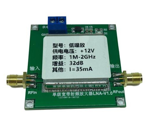
When searching for an LNA on Amazon or other e-commerce websites, you can easily find one simply named LNA V1.0 (with the tell-tale Chinese marking on the PCB: 单级宽带 频放大器 = Single stage broadband frequency amplifier). The LNA uses a SBB5089Z chip (datasheet) that seems to be fairly sensitive and powerful.
Sadly the circuit used is not perfect, and some shortcomings are present, some of which can also damage the chip. Let's see how we can mod the LNA to make it better!
Circuit description
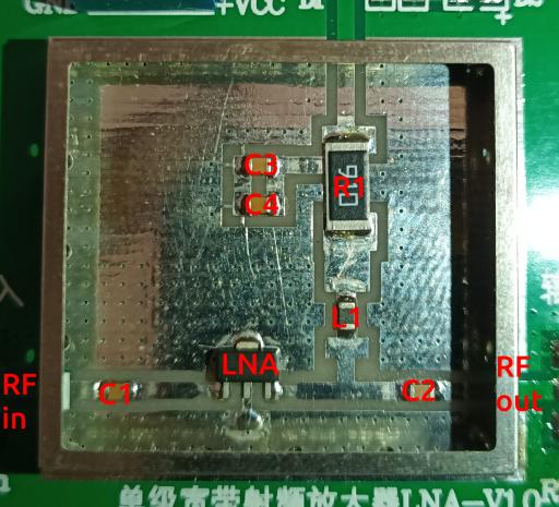
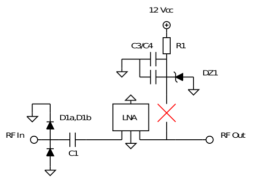
The circuit is very simple, but I have reverse engineered it here for clarity.

Here is the position of components on the PCB.
Power supply
The SBB5089Z is designed to work with 5 V, however as sold it requires 12 V to work. There is no voltage regulator on board, but a simple 91 ohm dropper resistor (R1). Of course, this is not an ideal solution, as if you try to supply the board with 13.8 V as commonly found in hamshacks, you will end up with 5.3 V at the chip, and the absolute maximum voltage is 5.5 V! This problem already caused the death of a board, so better find a solution!
To solve the problem, it is sufficient to add a 5.1 V Zener (DZ1 on the schematic) right after the dropper resistor R1, just before the filter inductance L1. Even if the input voltage rises above 12 V, the Zener will ensure it will never rise above 5.2-5.3V and thus it is impossible to damage the chip.

ESD protection
The chip is not meant to be connected directly to an antenna, so it does not feature any sort of ESD protection. We can however add our own, using a BAV99 double diode in SMD package (marked as D1a, D1b on the schematic) at the input, right before the coupling capacitor C1. It is also possible to add a neon bulb as an additional protection. It will act like a gas discharge tube, limiting the input spike to about 80 volts.
Of course it is possible to use other diodes, but care should be taken not to add excessive parasitic capacitances which will load the RF circuit and change its behavior. For instance, the classic 1N4007 diode should be avoided, as it has about 20pF of junction capacitance. As a comparison, the BAV99 only has 1 pF.

Bias Tee
The circuit is designed to be operated with a bias tee, but the board only features an internal one and has no provision for an external bias tee.
5 volt bias tee
Remove and short capacitor C2, and remove the L1 choke. The external bias tee will replace these two components. You can of course omit the DZ1 zener diode as it's not needed.
12 volt bias tee
This is a better idea if you are running a long coax cable, or your radio/SDR does not output 5 volts.
Add a choke of suitable value (read the datasheet, for frequencies below 500 MHz it suggests 330nH) between the RF output and the dropper resistor R1 (marked L2 on the schematic). Check the voltage, if it is below 5 volts replace R1 with a lower value.

Have fun with your modded LNA!